
|
Getting your Trinity Audio player ready...
|
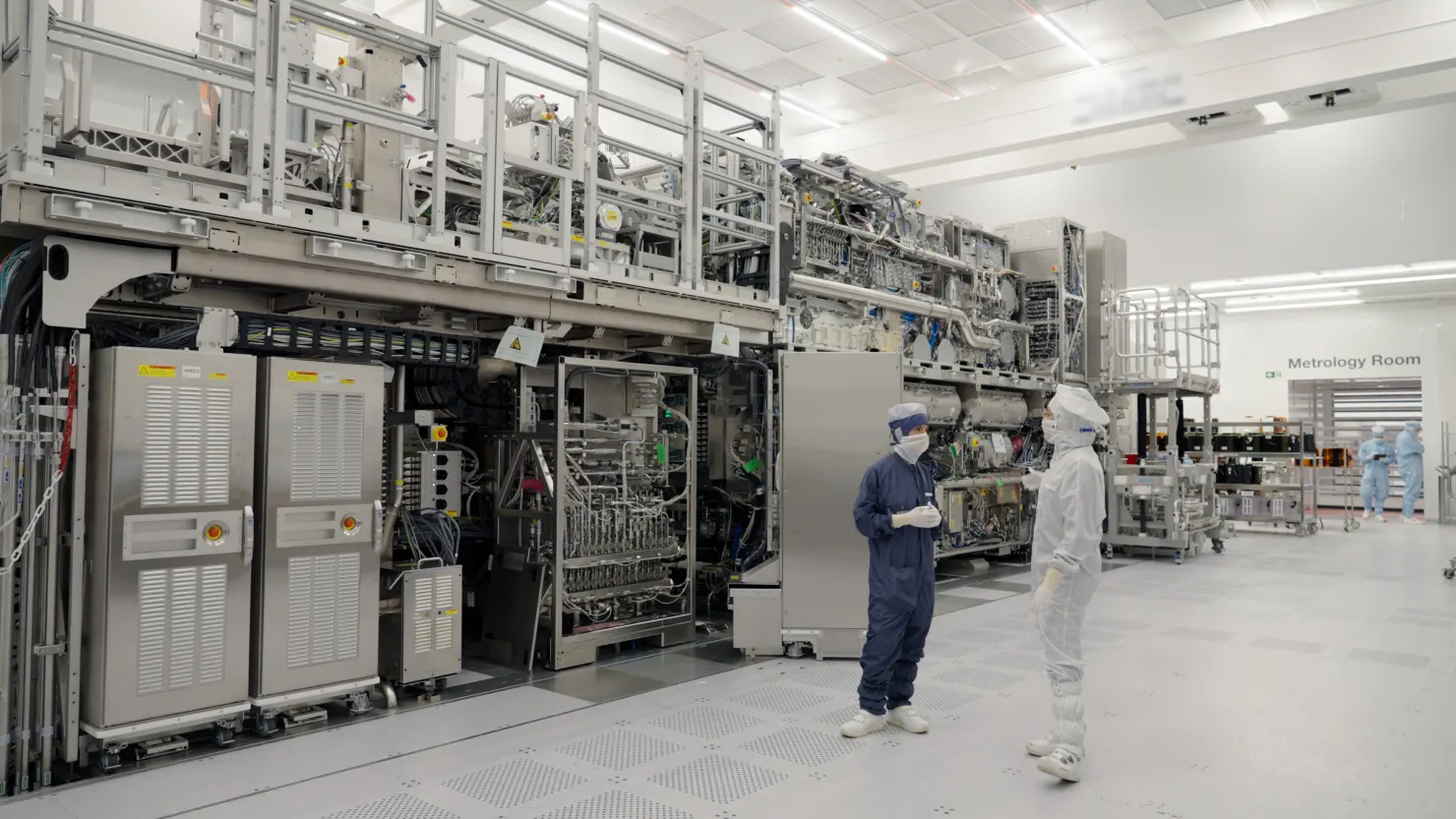
TSMC and Samsung, the world’s two largest chipmakers, have formally committed to adopting ASML’s High NA extreme ultraviolet lithography machines, ending a lengthy period of industry hesitation around one of the most expensive pieces of manufacturing equipment ever built. The announcement, confirmed Tuesday, gives ASML the broad customer commitment it has spent years pursuing, and it arrives as artificial intelligence demand pushes chipmakers to squeeze increasingly complex transistor architectures onto silicon at a pace that older lithography tools are struggling to keep up with.
To understand why this matters, it helps to know what these machines actually do. EUV lithography tools function as the printing press of the semiconductor industry, using extreme ultraviolet light to etch circuit patterns onto silicon wafers at scales measured in nanometers. ASML is the only company on Earth that manufactures this equipment, giving it an effective monopoly over one of the most critical bottlenecks in global chip production. High NA, the newest generation of that technology, pushes resolution even further than standard EUV tools, allowing chipmakers to pack significantly more transistors into the same physical space, a capability that’s become increasingly valuable as AI chip designs grow more transistor-dense with each new generation.
Under the newly confirmed timeline, Samsung plans to bring High NA EUV machines into high-volume manufacturing by 2028, starting specifically with DRAM memory production rather than its logic chip foundry business. TSMC, notably more cautious until now, has committed to adopting the technology for advanced chip production starting in 2030. Intel, meanwhile, has already been running production using High NA EUV tools, having reportedly processed more than a million wafers through the machines according to Tom’s Hardware, a volume that reportedly exceeds the rest of the industry combined. Each High NA machine costs approximately $400 million, a price tag that has been central to why TSMC in particular spent much of the past two years reportedly weighing cheaper alternatives, including photomask pellicles, rather than committing to ASML’s newest and most expensive equipment.
Alongside the adoption timeline, ASML, TSMC, Samsung, and Intel have also agreed to shift from six-inch photomasks to a larger 12-inch format, a change ASML says could boost production output by as much as 40 percent. That mask-size transition is being treated as a coordinated, multi-year industry roadmap rather than a single company’s decision, with the group targeting a 12-inch mask pilot production line by 2031 and full high-volume manufacturing readiness using 12-inch High NA EUV systems by 2033. SK Hynix is also reportedly evaluating participation in that same mask-size consortium specifically for DRAM production timed around 2028, and Belgian research institute Imec separately secured its own High NA EUV system back in March 2026, also priced at roughly $400 million, underscoring how the technology has begun spreading beyond the handful of dominant commercial chipmakers into research infrastructure as well.
Barclays framed Tuesday’s announcement as resolving one of the more persistent open questions hanging over ASML’s stock, telling clients in a note that the commitments “should provide more visibility on adoption which has been a key debate,” and characterizing the news overall as a positive development for the company. That framing matters given how directly ASML’s future growth trajectory depends on broad industry adoption of High NA specifically. ASML shares are up roughly 120 percent over the past twelve months, and investors have increasingly treated the pace of High NA commitments as a key signal for whether that run can continue, even though shares of the Amsterdam-listed company traded flat to slightly lower in early trading Tuesday despite the positive framing from analysts.
TSMC’s shift is arguably the more significant story buried within this announcement, given how publicly hesitant the company had been. As the world’s largest contract chipmaker and the manufacturer behind the vast majority of Nvidia’s most advanced AI GPUs, TSMC’s earlier reluctance to commit to High NA carried real weight across the broader semiconductor supply chain, since where TSMC goes, the industry’s collective manufacturing roadmap tends to follow. Intel, notably, missed out on the previous generation of EUV adoption years ago, a decision widely credited with helping TSMC pull ahead in the foundry race during the mid-2010s. By locking in a concrete 2030 adoption date now rather than continuing to hedge, TSMC appears to be deliberately avoiding a repeat of that earlier missed transition, even if it’s arriving to High NA later than Intel did.
Samsung’s decision to begin its own High NA rollout in memory production rather than its competing foundry business offers a useful window into the company’s broader strategic thinking. According to Samsung’s own newsroom materials, framing the 2028 rollout around DRAM scaling first suggests the company wants to prove out High NA’s precision advantages in memory manufacturing before committing the technology to the foundry operations that compete directly against TSMC for advanced logic chip customers, a more conservative sequencing than jumping straight into its highest-stakes competitive battleground.
The broader context here ties directly back to the AI boom reshaping demand across the entire chip manufacturing value chain. Nvidia’s dominance in AI hardware has drawn enormous attention, but none of that would be possible without TSMC, Samsung, and memory suppliers like SK Hynix and Micron actually manufacturing the underlying silicon, work that increasingly depends on ASML’s lithography monopoly sitting one layer further back in the supply chain. As Techzine’s analysis of the announcement put it, anyone building advanced chips ultimately needs ASML, and while reports have periodically surfaced about potential Chinese alternatives to EUV lithography, no credible competitor has yet emerged to challenge that monopoly position.
For the broader chip industry, Tuesday’s coordinated commitments effectively lock in a multi-year manufacturing roadmap that extends all the way through 2033, giving chip designers, AI hardware companies, and the broader technology supply chain a clearer sense of when the next meaningful jump in transistor density and manufacturing efficiency will actually arrive. Whether that timeline holds firm as AI demand continues evolving, or shifts again as it has multiple times over the past several years, will likely become one of the more closely watched storylines in semiconductor manufacturing heading into the back half of the decade.
Further technical detail on High NA EUV technology is available through ASML’s official newsroom. For more coverage of semiconductor manufacturing and AI infrastructure, visit Business Tech.