|
Getting your Trinity Audio player ready...
|
The race to build more powerful AI chips has increasingly shifted away from the transistors themselves and toward the packaging that connects them, and German laser and industrial technology company TRUMPF says it has cracked one of the toughest manufacturing problems standing in the way of that next generation of packaging. The company announced this week that it has developed what it describes as the first industrial process capable of reliably coating the millions of microscopic holes required for glass substrates, a packaging material widely seen as essential for scaling AI processors beyond the physical limits of today’s chip designs.
To understand why this matters, it helps to know why glass has become such a hot topic in chip packaging in the first place. As AI processors pack more computing power and memory into increasingly constrained physical spaces, overall system performance depends just as much on how efficiently different chip components, chiplets, memory, and interconnects, communicate with each other as it does on transistor design itself. Glass substrates are being explored specifically because they can support denser interconnects and faster, more efficient data transmission within these chip packages compared to the organic substrates the industry has relied on for years. TRUMPF’s Chief Technology Officer, Dr. Berthold Schmidt, laid out this reasoning at a press conference in Taipei, emphasizing that while transistor scaling remains necessary, future computing performance increasingly hinges on solving separate bottlenecks tied to data movement, power delivery, and thermal dissipation, areas where packaging innovation, not chip design alone, is now doing the heavy lifting.
Traditional organic substrates are genuinely reaching their limits as AI chip packages continue to grow in size. Under the high temperatures involved in chip assembly, larger packages become increasingly prone to warpage, a physical deformation that reduces manufacturing yield and gets progressively harder to control as package dimensions expand, according to semiconductor industry analysis from research firm TrendForce. Glass substrates offer better dimensional stability under these conditions, but manufacturing them at the precision and scale AI chip production actually requires has proven genuinely difficult, and that difficulty is exactly the problem TRUMPF says its new technology addresses.
The specific manufacturing challenge involves what the industry calls through-glass vias, essentially millions of extremely narrow, deep holes drilled through glass panels that then need to be coated with conductive metal to carry electrical signals through the substrate. TRUMPF’s own lasers can already drill these microscopic holes reliably, but Piotr Lach, who leads Next Technology Demands at TRUMPF Elektronik, identified the real bottleneck as achieving uniform, void-free conductive metallization deep inside these narrow, high-aspect-ratio holes. Getting that coating step wrong carries serious consequences for manufacturers, since even a relatively small number of incorrectly coated vias can render an entire glass panel unusable, a failure mode that becomes economically punishing once you’re trying to manufacture at the volume commercial chip production actually demands.
TRUMPF’s answer is a technology called High Power Impulse Magnetron Sputtering, or HiPIMS, which generates a highly ionized plasma that, combined with directional radio frequency bias controls, actively guides charged metal ions deep into these narrow cavities to form dense, uniform seed layers along the via sidewalls. In plainer terms, rather than relying on more conventional coating methods that struggle to deposit material evenly deep inside such narrow, high-aspect-ratio structures, TRUMPF’s plasma-based approach pushes metal ions directionally into the holes, achieving the kind of consistent coverage manufacturers need to hit acceptable production yields at genuine industrial scale. The company says this approach improves process stability and increases production yield compared to conventional coating methods, addressing precisely the reliability gap that has kept glass substrates largely confined to research and pilot programs rather than volume manufacturing up to this point.
TRUMPF isn’t approaching this in isolation, and the competitive and collaborative landscape around glass substrate manufacturing gives useful context for how significant this development actually is. The company has reportedly worked alongside SCHMID Group on integrating laser drilling with downstream etching and wet processing steps needed to make finished glass substrates usable, an approach SCHMID says can shorten overall process times by roughly a factor of ten compared to less integrated workflows. Other players are pursuing different technical routes toward the same underlying goal, including Taiwan-based E&R Engineering, whose E-Core System alliance claims a laser-modification platform capable of processing up to 8,000 vias per second for fixed matrix patterns, while German competitor LPKF has reported that more than 80 percent of customers preparing glass and advanced packaging production ramps are already qualifying equipment with LPKF specifically, though that activity has not yet translated into volume revenue for the sector broadly. That competitive backdrop suggests glass substrate manufacturing technology remains genuinely unsettled territory, with multiple companies racing toward viable industrial processes rather than any single approach having already emerged as the clear industry standard.
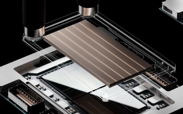
TRUMPF plans to showcase this HiPIMS technology, alongside a broader AI hardware roadmap that includes tripled EUV lithography capacity and direct in-chip cooling structures, at SEMICON Taiwan 2026, one of the semiconductor industry’s most closely watched annual trade events. The company’s broader technology portfolio spanning ultrashort-pulse lasers for creating the initial via structures, plasma power supplies for coating, and etching capabilities positions TRUMPF to address multiple stages of the glass substrate manufacturing process rather than a single isolated step, an integrated approach that could prove commercially significant if chip manufacturers prefer sourcing more of this specialized equipment from a single vendor rather than piecing together solutions from multiple suppliers.
Demand for advanced packaging technology broadly is climbing steadily alongside the ongoing buildout of AI data centers and high-performance computing infrastructure worldwide, a trend that shows no signs of slowing given how much capital continues flowing into AI compute capacity globally. Still, exactly how quickly glass substrates move from promising research technology into mainstream, high-volume chip production remains genuinely uncertain, dependent on factors ranging from continued yield improvements to whether major chip manufacturers and foundries decide the performance benefits justify the cost and complexity of shifting away from decades of accumulated organic substrate manufacturing expertise. TRUMPF’s HiPIMS announcement represents a meaningful technical step toward solving one specific, well-documented bottleneck standing in that path, though the broader transition toward glass-based AI chip packaging will likely unfold gradually over the coming years rather than arriving as a single decisive breakthrough moment.
Further technical detail on TRUMPF’s semiconductor manufacturing technology is available through the company’s official press materials. For more coverage of AI chip manufacturing and semiconductor infrastructure, visit Business Tech.